The semiconductor industry has been at the forefront of technological advancements, powering innovations in various fields. In recent years, the demand for smaller, faster, and more powerful electronic devices has surged, driving semiconductor manufacturers to seek higher efficiency and precision in their processes. As a result, wafer handling automation has become a critical aspect of semiconductor manufacturing, and automated wafer handling robots have emerged as indispensable tools in the industry. In this blog, we will explore the wafer handling robots market from three crucial aspects: the rise of automated wafer handling, the significance of semiconductor wafer handling robots, and the market's projection for the future.
The Rise of Automated Wafer Handling
In semiconductor manufacturing, wafers act as the foundation for building microchips and other electronic components. These wafers are extremely delicate and expensive, often requiring a cleanroom environment to avoid contamination. Traditional manual handling of wafers poses a significant risk of damage and contamination, leading to potential yield losses and increased production costs.
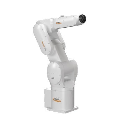
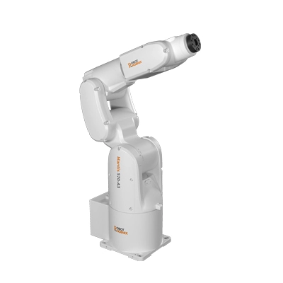
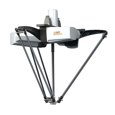
Automated wafer handling systems have stepped in to address these challenges. Wafer handling robots are specialized machines designed to safely transport and process wafers throughout various stages of production. These robots offer several key advantages over manual handling:
Precision and Consistency: Wafer handling robots can consistently handle wafers with high precision, reducing the risk of errors and minimizing defects during the manufacturing process. This level of accuracy ensures uniformity in the final product, leading to higher-quality semiconductor devices.
Cleanroom Compatibility: Semiconductor wafer handling robots are designed to operate within cleanroom environments, maintaining the necessary levels of cleanliness and preventing contamination. This is essential for producing reliable and defect-free chips.
Increased Throughput: Wafer handling automation significantly improves the overall throughput of semiconductor fabs. Robots can efficiently move wafers between tools and processes, reducing cycle times and enhancing productivity.
The Significance of Semiconductor Wafer Handling Robots
The semiconductor wafer handling robots market is witnessing substantial growth, primarily driven by the following factors:
Technological Advancements: The rapid evolution of robotics and automation technology has enabled the development of highly sophisticated wafer handling robots. These robots can handle wafers of various sizes and materials, supporting the diverse needs of semiconductor manufacturers.
Cost-Effectiveness: While the initial investment in wafer handling robots may be substantial, the long-term cost benefits outweigh the initial expenditure. Automated handling reduces the need for manual labor, resulting in cost savings, increased production efficiency, and reduced waste.
Industry 4.0 Integration: As the semiconductor industry embraces Industry 4.0 principles, wafer handling robots play a crucial role in creating interconnected and data-driven manufacturing environments. These robots are often equipped with sensors and data analytics capabilities, enabling predictive maintenance and optimized production scheduling.
Minimized Human Intervention: By automating wafer handling, manufacturers can minimize human intervention in the production process. This, in turn, reduces the risk of human errors, ensures consistent quality, and enhances safety for workers in cleanroom environments.
Rising Demand for Semiconductors: The increasing demand for semiconductor chips in various industries, such as automotive, consumer electronics, and healthcare, is driving semiconductor manufacturers to expand their production capacities. Wafer handling robots enable these manufacturers to scale their operations efficiently.
Market Projection for the Future
The wafer handling robots market is poised for significant growth in the coming years. Several factors contribute to the positive market outlook:
Miniaturization and Advanced Packaging: The trend towards smaller and more powerful electronic devices has led to the development of advanced packaging techniques. Wafer handling robots are crucial in handling thinner wafers and complex packaging processes required for advanced semiconductor packaging.
Emergence of 5G Technology: The deployment of 5G technology and the increasing demand for data-intensive applications are spurring the need for advanced semiconductors. Wafer handling robots will play a key role in meeting the production demands of 5G-enabled devices.
Internet of Things (IoT) and AI Integration: The integration of IoT and AI technologies with wafer handling robots will further enhance their capabilities. These robots will be capable of making real-time decisions, optimizing production workflows, and improving overall equipment efficiency.
Regional Market Growth: The Asia-Pacific region, especially China, South Korea, and Taiwan, has been a major hub for semiconductor manufacturing. The demand for wafer robots in this region is expected to remain strong due to increased investments in semiconductor fabs.
Sustainable Manufacturing Practices: The semiconductor industry is becoming increasingly focused on sustainability. Wafer handling robots can contribute to this goal by optimizing energy consumption, reducing waste, and improving resource utilization.
The wafer handling robots market is at the forefront of the semiconductor industry's transformation towards automation and efficiency. As automated wafer handling becomes an integral part of semiconductor manufacturing, the industry can expect improved productivity, reduced production costs, and enhanced product quality. With advancements in robotics and smart manufacturing technologies, semiconductor wafer handling robots are set to play a pivotal role in meeting the demand for cutting-edge electronic devices and driving innovation in the semiconductor sector for years to come.
Comprehensive Guide to Industrial Robotic Automation
 Learn More
 EN
EN  ja
ja  ko
ko  fr
fr  de
de  es
es  ru
ru  pt
pt  ar
ar  vi
vi  ur
ur 


